
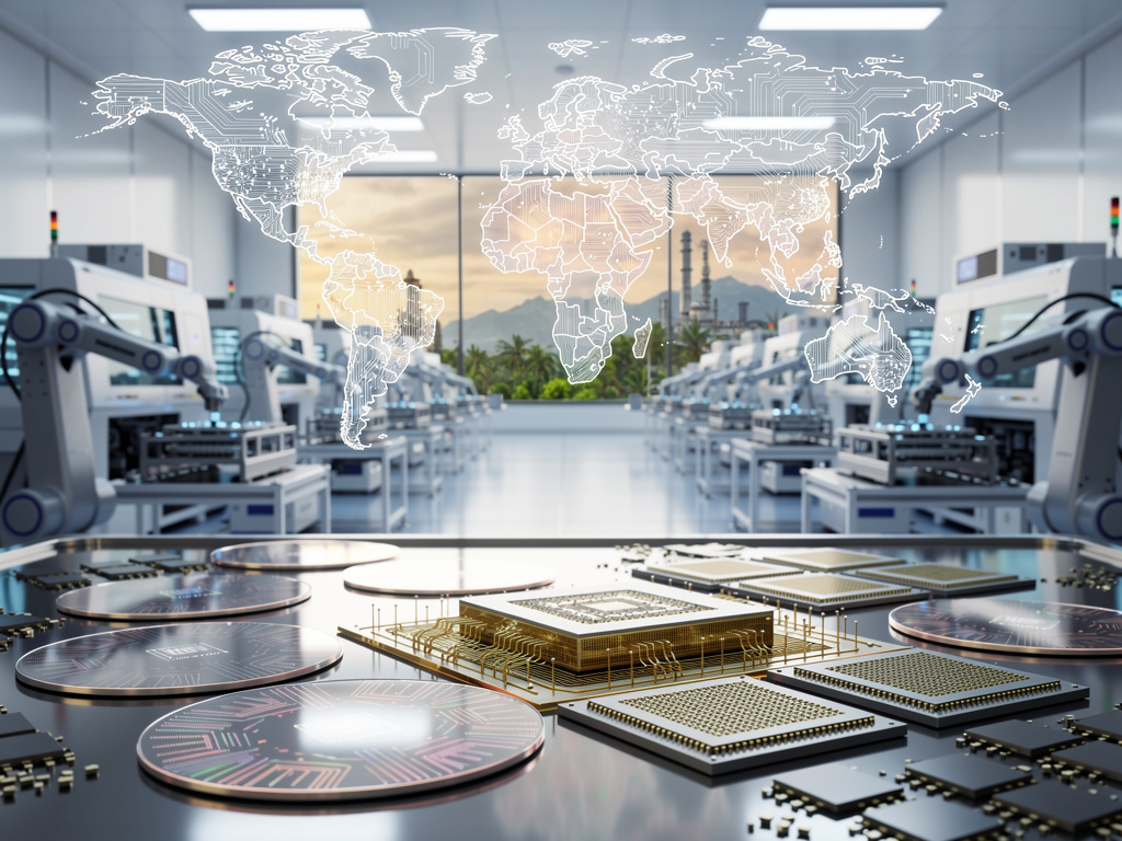
Samsung Electronics is doubling down on Vietnam — and the stakes are enormous. The South Korean conglomerate recently committed to investing roughly $1.8 billion to build an advanced semiconductor packaging facility in the northern Vietnamese province of Bac Ninh, a move that reshapes the company’s manufacturing footprint and sends a clear message about where the future of chip production is heading. Not just for Samsung. For everyone.
The investment, first reported by TechRepublic, represents Samsung’s largest single capital commitment in Vietnam’s semiconductor sector and will focus on advanced packaging — the increasingly critical final stage of chip manufacturing where individual dies are assembled, interconnected, and prepared for integration into devices. It’s the part of the process that has quietly become one of the most important bottlenecks in the global supply chain.
Why Vietnam? Why now? And why packaging specifically? The answers reveal a convergence of geopolitical calculation, technical necessity, and cold economic logic that is redrawing the map of global semiconductor manufacturing.
Samsung has operated in Vietnam for over a decade. The company already runs massive smartphone and electronics assembly operations in the country, employing hundreds of thousands of workers across facilities in Bac Ninh and Thai Nguyen provinces. Vietnam has been central to Samsung’s consumer electronics supply chain for years, but semiconductor manufacturing is a different animal entirely. The new facility marks a significant escalation in the complexity and strategic importance of Samsung’s Vietnamese operations.
Advanced packaging has emerged as one of the most contested territories in the chip industry. For decades, the spotlight fell almost exclusively on the fabrication of transistors — shrinking them ever smaller on silicon wafers in the relentless pursuit of Moore’s Law. That pursuit hasn’t stopped, but the industry has increasingly recognized that how chips are assembled and connected matters almost as much as how small the transistors are. Technologies like chiplets, 2.5D and 3D stacking, fan-out wafer-level packaging, and hybrid bonding have transformed packaging from an afterthought into a strategic differentiator.
Taiwan Semiconductor Manufacturing Company (TSMC) has poured billions into its own advanced packaging capabilities, most notably its CoWoS (Chip-on-Wafer-on-Substrate) platform, which has become essential for packaging Nvidia’s AI accelerators. The demand for CoWoS capacity has been so intense that it has created supply constraints affecting the entire AI hardware market. Samsung, which competes with TSMC in both foundry services and packaging, can’t afford to fall behind.
So the Vietnam investment isn’t just about finding cheaper labor or diversifying geographically. It’s about building capacity in a segment of the semiconductor value chain where demand is surging and where Samsung needs scale to remain competitive against TSMC and Intel.
The geopolitical dimension is impossible to ignore. The U.S.-China trade war, now in its seventh year under successive administrations, has fundamentally altered how multinational corporations think about manufacturing concentration. The semiconductor industry, in particular, has been caught in the crossfire. Export controls targeting China’s access to advanced chip technology, tariffs, and the CHIPS Act’s incentives for domestic U.S. production have all contributed to a global reshuffling of supply chains.
Vietnam sits in a sweet spot. It’s not China, which means companies can avoid the worst of the tariff and export control complications. It’s geographically proximate to existing Asian supply chains. Labor costs are competitive. And the Vietnamese government has been aggressively courting semiconductor investment with tax incentives, infrastructure development, and workforce training programs.
According to Reuters, Vietnam has been positioning itself as a viable alternative to China for technology manufacturing, and Samsung’s investment validates that strategy in a major way. The country has also attracted interest from Intel, which operates a significant packaging and testing facility in Ho Chi Minh City, and from various other chip companies evaluating Southeast Asian locations for new capacity.
But Vietnam faces real challenges. The country’s semiconductor workforce is still developing. Advanced packaging requires engineers and technicians with specialized skills in areas like thermal management, signal integrity, and precision bonding — expertise that takes years to cultivate. Samsung will need to invest heavily in training, and the Vietnamese education system will need to continue scaling up its technical programs to meet the demand.
Infrastructure is another concern. Semiconductor manufacturing, even at the packaging stage, requires extraordinarily reliable power, water, and logistics networks. Vietnam has made significant progress on infrastructure in recent years, but sustained investment will be necessary to support the kind of high-volume, high-precision manufacturing that advanced packaging demands.
None of this has deterred Samsung. The company appears to have concluded that the strategic benefits outweigh the operational risks. And there’s a broader pattern here. Samsung has been systematically expanding its semiconductor operations beyond South Korea, with investments in Taylor, Texas (a $17 billion fab), and now this major packaging facility in Vietnam. The company is building a geographically distributed manufacturing network that hedges against regional disruptions — whether from natural disasters, geopolitical conflicts, or trade policy shifts.
This approach mirrors what TSMC has been doing with its Arizona fabs and its planned facilities in Japan and Germany. Intel, too, is expanding globally with new fabs in Ohio, Germany, and Israel. The era of hyper-concentrated semiconductor manufacturing is ending. Not overnight. But the trajectory is clear.
The timing of Samsung’s announcement also coincides with intensifying competition in the AI chip market, where packaging technology has become a critical enabler. Nvidia’s next-generation GPU architectures, AMD’s MI300 series, and various custom AI accelerators from hyperscalers like Google, Amazon, and Microsoft all rely on advanced packaging to achieve the performance, power efficiency, and memory bandwidth that AI workloads demand. Every major chip company is scrambling for packaging capacity, and Samsung’s Vietnam facility is positioned to serve that growing demand.
Samsung’s own AI chip ambitions add another layer. The company has been working to win back foundry customers and capture a larger share of the AI accelerator market, both through its foundry services and through its own HBM (High Bandwidth Memory) products. HBM, which stacks multiple DRAM dies using through-silicon vias, is itself an advanced packaging technology. Samsung has faced quality and yield challenges with its HBM products — issues that contributed to Nvidia reportedly favoring SK Hynix as a supplier — and expanding its packaging capabilities could help address those problems.
The $1.8 billion figure, while substantial, is just one piece of Samsung’s broader capital expenditure strategy. The company spent approximately $36 billion on capital expenditures in 2023, with a significant portion directed toward its semiconductor division. The Vietnam investment represents a targeted bet on a specific capability — packaging — rather than a comprehensive buildout of front-end fabrication capacity. That distinction matters. Front-end fabs, where wafers are actually processed, cost $15-20 billion or more to build. Packaging facilities are less capital-intensive but increasingly strategic.
For Vietnam, the investment carries implications that extend well beyond Samsung’s balance sheet. A major advanced packaging facility will create thousands of jobs, stimulate the development of a local supplier base, and accelerate the country’s integration into the highest-value segments of the global semiconductor supply chain. It could also attract additional investment from other chip companies looking to co-locate near a major player like Samsung.
There’s a multiplier effect at work. When a company like Samsung builds a semiconductor facility, it doesn’t operate in isolation. Equipment suppliers, materials companies, logistics providers, and testing firms all follow. The result is a cluster of related businesses that collectively strengthen the region’s capabilities and attractiveness for further investment. Bac Ninh could become for Vietnam what Hsinchu is for Taiwan — a concentrated hub of semiconductor expertise and activity.
That’s the optimistic scenario. The pessimistic one involves the familiar risks: execution delays, cost overruns, geopolitical shifts that alter the calculus, or a cyclical downturn in the semiconductor market that forces companies to scale back investment plans. Samsung itself has experienced some of these challenges with its Taylor, Texas fab, which has faced delays and workforce difficulties.
Still, the structural forces driving this investment are powerful and unlikely to reverse. The demand for advanced packaging is growing faster than the demand for leading-edge fabrication nodes. AI is consuming packaging capacity at an unprecedented rate. And the geopolitical incentives to diversify manufacturing away from any single country or region have never been stronger.
Samsung’s Vietnam bet is, at its core, a recognition that the semiconductor industry’s center of gravity is shifting — not from one country to another, but from concentration to distribution, from fabrication dominance to packaging parity, and from purely technical competition to a contest that spans economics, geopolitics, and industrial strategy simultaneously.
The chips are being placed. Literally and figuratively. And Vietnam, a country that just a decade ago was primarily known in the tech world for assembling smartphones, is now positioned at the center of one of the most consequential industrial transitions of the 21st century.


 WebProNews is an iEntry Publication