
Samsung Electronics has officially entered a new chapter in the artificial intelligence hardware arms race. On Thursday, the South Korean semiconductor giant announced it had begun mass production of its next-generation High Bandwidth Memory (HBM) chips — a move that signals both a technological leap forward and a strategic bid to reclaim ground lost to rival SK Hynix in one of the most consequential battles in the global chip industry.
The announcement, first reported by The Daily Journal via the Associated Press, marks the beginning of volume production for Samsung’s HBM4 chips — the latest iteration of specialized memory designed to handle the enormous data throughput demands of AI training and inference workloads. These chips are critical components in the accelerator cards and GPU systems manufactured by companies like Nvidia, which dominate the data center infrastructure powering generative AI applications from ChatGPT to autonomous driving systems.
What HBM4 Means for the AI Hardware Supply Chain
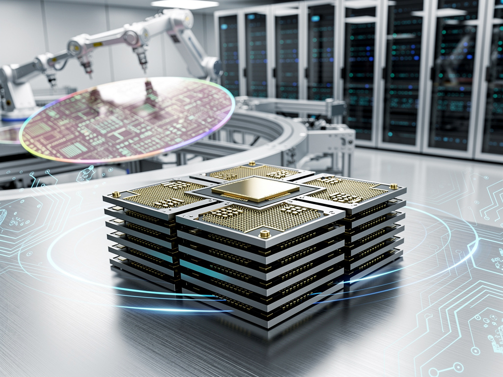
High Bandwidth Memory is not a new concept, but its importance has surged dramatically over the past two years as the AI boom has reshaped semiconductor demand curves. HBM chips are stacked vertically — multiple layers of DRAM dies connected by thousands of tiny through-silicon vias (TSVs) — enabling data transfer rates that far exceed those of conventional memory. Each successive generation has pushed the envelope on bandwidth, capacity, and energy efficiency, and HBM4 represents the most ambitious step yet.
Samsung’s HBM4 chips are expected to deliver significantly higher bandwidth and greater memory capacity per stack compared to the current HBM3E generation. Industry analysts have noted that HBM4 is designed to meet the requirements of next-generation AI accelerators that will begin shipping in 2025 and 2026, including anticipated future products from Nvidia and AMD. The timing of Samsung’s mass production announcement is therefore not incidental — it is a calculated effort to position the company as a first mover in supplying what could become the most in-demand semiconductor component of the next several years.
Samsung’s Uphill Battle Against SK Hynix
For all the fanfare surrounding the announcement, Samsung’s move comes against a backdrop of competitive pressure that has been, by the company’s own admission, uncomfortable. SK Hynix, Samsung’s smaller but fiercely competitive South Korean rival, has dominated the HBM market in recent years. SK Hynix was the first to mass-produce HBM3 and HBM3E chips, and it secured the lion’s share of supply agreements with Nvidia — the single most important customer in the AI chip ecosystem. By some industry estimates, SK Hynix held roughly 50% or more of the HBM market in 2024, with Samsung trailing and Micron Technology of the United States holding a smaller but growing share.
Samsung’s difficulties with HBM3E qualification — the process by which Nvidia and other customers validate that memory chips meet their stringent performance and reliability standards — were widely reported throughout 2024. Delays in passing Nvidia’s qualification tests meant lost revenue and market share at precisely the moment when demand was exploding. The company’s semiconductor division posted disappointing earnings relative to expectations, and Samsung’s leadership publicly acknowledged the need to accelerate its HBM roadmap. The mass production of HBM4 can thus be read as Samsung’s attempt to leapfrog the current generation and establish a foothold in the next one before SK Hynix can consolidate its advantage.
The Technical Architecture Behind the New Chips
HBM4 introduces several architectural changes that distinguish it from its predecessors. The JEDEC Solid State Technology Association, the industry body that sets memory standards, finalized the HBM4 specification to allow for a wider interface — moving from a 1,024-bit interface in HBM3 and HBM3E to a 2,048-bit interface in HBM4. This doubling of the interface width is a fundamental change that enables a proportional increase in data throughput, assuming other system-level bottlenecks can be managed.
Samsung has indicated that its HBM4 products will feature 12-high stacks — meaning 12 individual DRAM dies stacked vertically in a single package. The company has invested heavily in advanced packaging technologies, including its proprietary hybrid copper bonding techniques, which allow for finer-pitch interconnects between die layers. This is critical because as stacks grow taller, the thermal and electrical challenges multiply. Heat dissipation becomes a primary engineering concern, and Samsung has touted improvements in thermal management as a key differentiator for its HBM4 products.
Why Memory Has Become the Bottleneck in AI Computing
The centrality of HBM to the AI revolution cannot be overstated. Modern large language models — the kind that power OpenAI’s GPT series, Google’s Gemini, and Meta’s Llama — contain hundreds of billions of parameters. Training these models requires moving vast quantities of data between processors and memory at speeds that conventional DDR5 DRAM simply cannot achieve. HBM solves this by placing the memory physically closer to the processor on an interposer or within an advanced package, dramatically reducing latency and increasing bandwidth.
Nvidia’s current-generation H200 and next-generation B200 GPUs rely on HBM3E, with each accelerator card incorporating multiple HBM stacks. As models continue to scale — and as inference workloads grow to dwarf training workloads in aggregate compute demand — the appetite for faster, denser memory will only intensify. Industry forecasters project that the total addressable market for HBM will grow from roughly $16 billion in 2024 to more than $100 billion by 2030, making it one of the fastest-growing segments in the entire semiconductor industry.
The Geopolitical Dimension of Memory Chip Manufacturing
Samsung’s announcement also carries geopolitical significance. The production of advanced HBM chips is concentrated almost entirely in South Korea, with Samsung and SK Hynix together accounting for the vast majority of global output. Micron, headquartered in Boise, Idaho, is the only non-Korean producer with serious HBM ambitions, and it remains a distant third in market share. This concentration of supply in a single country — one that sits in a volatile geopolitical neighborhood, with North Korea to its north and China across the Yellow Sea — has drawn increasing attention from policymakers in Washington, Brussels, and Tokyo.
The U.S. CHIPS and Science Act, signed into law in 2022, has directed tens of billions of dollars toward domestic semiconductor manufacturing, but the vast majority of those investments have targeted logic chips (processors) rather than memory. Samsung itself has committed to building new fabrication facilities in Taylor, Texas, though those plants are primarily focused on foundry services for logic chips rather than memory production. The question of whether the West has a strategic vulnerability in its dependence on Korean HBM supply is one that defense and trade officials are quietly but actively debating.
What Comes Next: The Road to HBM4E and Beyond
Samsung’s mass production of HBM4 is not the end of the road — it is more accurately the beginning of a new product cycle that will see rapid iteration. The company and its competitors are already working on HBM4E, an enhanced version that will push bandwidth and capacity even further. SK Hynix has publicly discussed its own HBM4 timeline, and Micron has signaled its intent to remain competitive in the space. The race is not merely about who can produce the fastest chip, but who can produce it at scale, with acceptable yields, and with the thermal and reliability characteristics that customers like Nvidia demand.
For Samsung, the stakes extend beyond the memory division. The company’s broader semiconductor business — including its foundry operations, which compete with TSMC for logic chip manufacturing contracts — has been under pressure. A strong showing in HBM4 could restore confidence among investors and customers alike, and it could provide the revenue and margin uplift that Samsung needs to fund its broader technology ambitions. Conversely, another stumble in qualification or yield could deepen the perception that Samsung has lost its edge in the memory business it once dominated without question.
A Defining Moment for Samsung and the Industry
The mass production of HBM4 chips is more than a product launch — it is a bellwether for the trajectory of the AI hardware industry. The companies that control the supply of these tiny, extraordinarily complex memory stacks will wield enormous influence over the pace and direction of AI development. Samsung’s announcement is a declaration of intent: it means to be one of those companies. Whether it can execute on that ambition, in the face of fierce competition and unforgiving technical demands, will be one of the defining stories in the semiconductor industry over the next several years.
As reported by the Associated Press, Samsung’s move underscores the breakneck speed at which the AI chip market is evolving. For industry insiders, the message is clear: the memory wars are far from over, and the next generation has already begun.

