
In the high-stakes world of semiconductor manufacturing, where precision at the atomic scale dictates global technological supremacy, a small San Francisco startup named Substrate has emerged from stealth mode with a provocative claim: it has developed a chipmaking tool that can rival the most advanced lithography equipment produced by Dutch giant ASML. Founded in 2022, Substrate is not just aiming to compete in toolmaking but harbors ambitions to establish a U.S.-based foundry that could challenge Taiwan Semiconductor Manufacturing Co. (TSMC), the undisputed leader in contract chip production. This bold move comes at a time when geopolitical tensions and supply chain vulnerabilities have thrust domestic chip production into the spotlight.
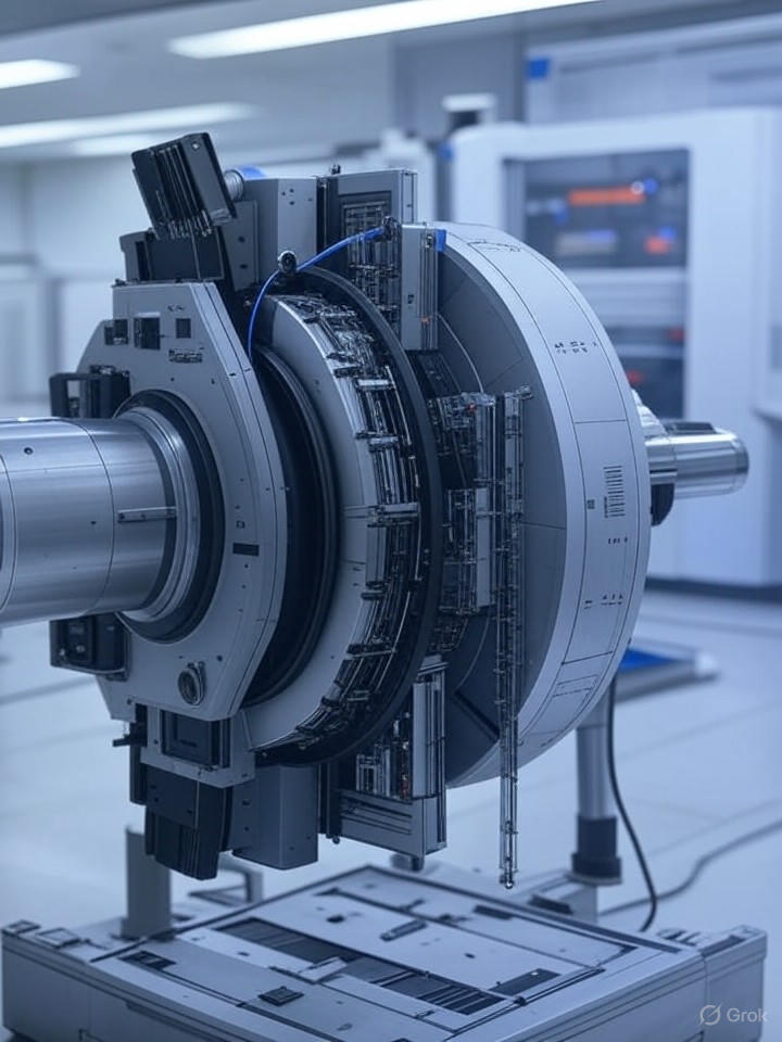
Substrate’s innovation centers on a novel approach to lithography, the critical process of etching intricate patterns onto silicon wafers. Unlike ASML’s extreme ultraviolet (EUV) systems, which rely on complex optics and lasers to produce wavelengths around 13.5 nanometers, Substrate employs compact particle accelerators to generate X-rays for lithography. According to a report by Reuters, this technology promises to enable production of chips at 2-nanometer scales and beyond, potentially at a fraction of the cost. CEO James Proud told Reuters in an interview that the company’s tool could slash manufacturing expenses by producing equipment much more cheaply than rivals.
From Stealth to Spotlight
Substrate’s announcement in late October 2025 sent ripples through the industry. The startup revealed it had raised over $100 million from prominent investors, including Peter Thiel’s Founders Fund, General Catalyst, and Valor Equity Partners, achieving a valuation exceeding $1 billion. As detailed in a Bloomberg article, Substrate’s particle accelerator-powered lithography machine represents a significant departure from established methods. Proud explained that by channeling light from a giant particle accelerator through a car-sized tool, the company could cut chipmaking costs in half.
The technology draws on X-ray lithography, a concept explored in the 1980s but largely abandoned due to challenges in generating sufficient X-ray intensity without enormous infrastructure. Substrate claims to have overcome these hurdles with custom-designed accelerators that are compact and efficient. Posts on X (formerly Twitter) from industry figures like Lulu Cheng Meservey highlighted actual patterns printed on silicon wafers using this method, emphasizing its potential to restore U.S. semiconductor dominance.
Technical Breakthroughs and Bold Claims
At the heart of Substrate’s pitch is the promise of superior resolution and cost efficiency. Tom’s Hardware reported that the startup’s X-ray system could surpass ASML’s EUV scanners by operating at shorter wavelengths, enabling finer features on chips. An analyst quoted in the piece noted that if successful, this could reduce wafer costs tenfold by the end of the decade. However, the same report scrutinized Substrate’s claims, with one analyst likening the venture to a fraud due to inconsistencies in technical messaging and leadership backgrounds.
Despite the skepticism, Substrate has demonstrated tangible results. Dylan Patel, a semiconductor analyst posting on X, acknowledged that the company has shown ‘pretty incredible results with their tool,’ though he raised open questions about scalability. The startup’s approach involves not selling the tools outright but integrating them into its own foundries, a strategy that Proud believes will allow Substrate to control the entire production process and undercut competitors.
Skepticism and Industry Hurdles
Critics argue that Substrate’s ambitions may be overstated. A deep dive by SemiAnalysis, referenced in X posts, pointed out that while the starting point isn’t zero, replicating the ecosystem built by ASML and TSMC— which includes decades of R&D, supplier networks, and intellectual property— is a monumental task. ASML’s EUV machines, for instance, cost hundreds of millions of dollars each and require specialized facilities, as noted in a New York Times article questioning whether a startup can truly make chips cheaper than industry giants.
Moreover, Substrate’s plan to build its own fabs adds another layer of complexity. TSMC is investing $100 billion in U.S. facilities, according to TradingView News, underscoring the scale required. Proud, however, remains undeterred. In an interview with Bloomberg TV, he described the company’s mission as creating an American alternative to foreign dominance in chip production, especially for advanced AI chips.
Investor Backing and Geopolitical Context
The influx of venture capital reflects broader enthusiasm for domestic semiconductor innovation amid U.S.-China tensions. Investors like Peter Thiel see Substrate as a strategic play to reduce reliance on Taiwan and the Netherlands. A Finance Yahoo piece highlighted how Silicon Valley heavyweights are betting on Substrate to ‘outrun TSMC and ASML,’ with the startup’s secretive development adding to its allure.
Yet, execution risks loom large. Building a foundry capable of producing cutting-edge chips requires not just advanced tools but also expertise in materials science, process engineering, and yield optimization. As Bits&Chips reported, Substrate aims to rival ASML’s EUV tools while challenging TSMC’s fabs, a dual assault that has drawn both admiration and doubt from industry observers.
Potential Impact on Global Supply Chains
If Substrate succeeds, it could reshape the semiconductor landscape. The company’s cost-reduction claims—potentially producing chips at a tenth of current expenses—might democratize access to advanced computing, accelerating AI and other technologies. Recent X posts from users like Wall St Engine noted the $100 million raise and $1 billion valuation, positioning Substrate as a key player in the push for U.S. chip sovereignty.
However, challenges such as regulatory hurdles, talent acquisition, and technological validation remain. Substrate is actively hiring, as mentioned in X updates from Lulu Cheng Meservey, signaling rapid expansion. Analysts from Tom’s Hardware and others warn that without transparent demonstrations, the startup’s claims could falter under scrutiny.
Looking Ahead in Semiconductor Innovation
As the industry watches, Substrate’s progress will be closely monitored. Comparisons to past disruptors abound, but the barriers in chipmaking are notoriously high. A US News article echoed the startup’s ambitious plan, while emphasizing the need for concrete proof. With demonstrations already underway, the coming months could determine if Substrate’s particle-powered vision becomes reality or joins the annals of overhyped tech ventures.
In an era where chips power everything from smartphones to supercomputers, Substrate’s challenge to ASML and TSMC underscores the relentless drive for innovation. Whether it succeeds or stumbles, the startup’s emergence highlights the dynamic, high-risk nature of the semiconductor frontier.

