
Intel’s Bold Leap: CEO Lip-Bu Tan Bets Big on 14A to Reclaim Semiconductor Supremacy
In the high-stakes world of semiconductor manufacturing, Intel Corp. is charting an ambitious course with its 14A process technology, a move that could redefine its position in a fiercely competitive industry. At the Consumer Electronics Show in Las Vegas this January, Intel’s Chief Executive Officer Lip-Bu Tan declared the company is “going big time into 14A,” signaling a major push into this advanced node expected to enter production by 2027. This announcement comes amid Intel’s efforts to recover from past manufacturing setbacks and challenge rivals like Taiwan Semiconductor Manufacturing Co. and Samsung Electronics Co.
Tan’s comments, made during a press Q&A session, highlighted the progress on 14A, noting strong yields and intellectual property momentum. He hinted at external customer interest, suggesting that early versions of the process design kit would be available to partners soon. This development is crucial for Intel’s foundry ambitions, as attracting third-party clients is key to scaling production and recouping massive investments in cutting-edge fabs.
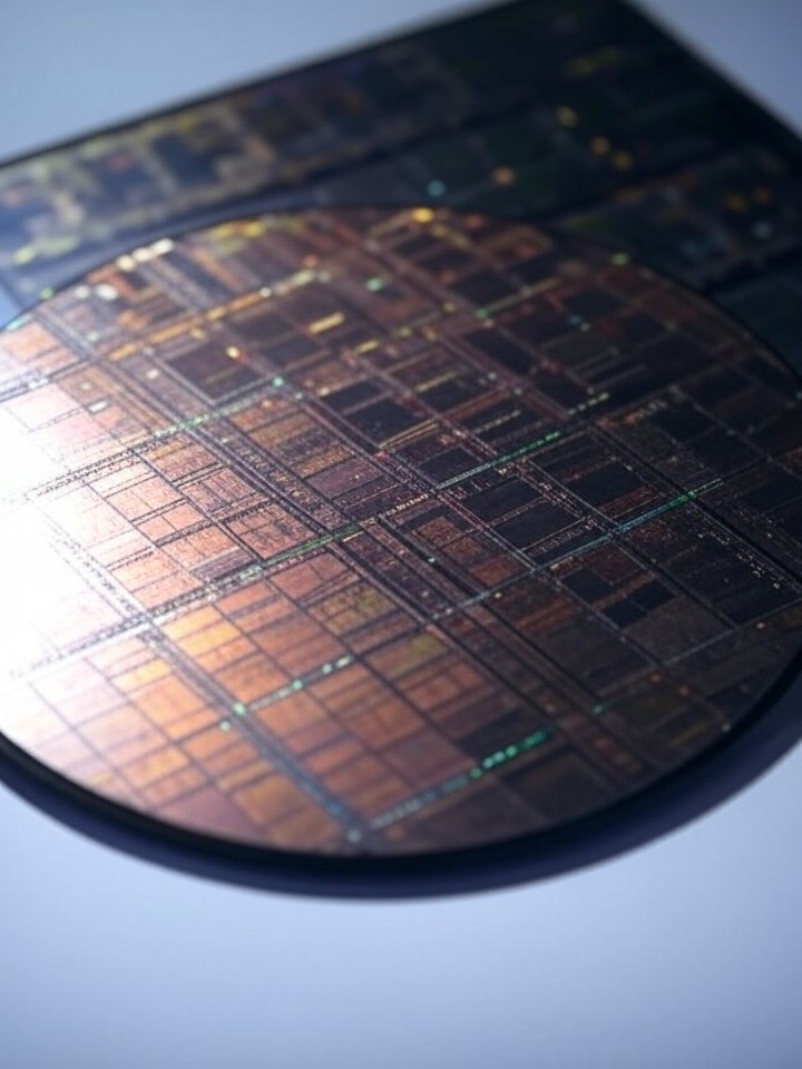
The 14A node represents a significant evolution from Intel’s current 18A process, which powers the newly unveiled Panther Lake processors. Building on innovations like RibbonFET transistors and PowerVia backside power delivery, 14A aims to deliver even greater density and efficiency. Industry observers see this as Intel’s bid to leapfrog competitors in the race to sub-2-nanometer technologies.
Advancements in Lithography and Node Scaling
Intel’s embrace of 14A incorporates High-NA extreme ultraviolet lithography, a technology that promises finer feature sizes and improved chip density. According to posts found on X, Intel has confirmed that 14A will be the world’s first process node to deploy High-NA EUV commercially, with tools already installed and exceeding performance targets. This follows Intel’s installation of the industry’s first commercial High-NA EUV tool, as reported in various tech outlets.
The company’s confidence stems from recent successes with 18A, where Tan claimed Intel “over-delivered” on timelines, shipping initial products ahead of schedule. At CES 2026, Intel showcased Panther Lake chips built on 18A, boasting 15% better performance-per-watt and up to 30% improved density compared to prior nodes. These metrics underscore the foundational technologies that will carry over to 14A.
However, challenges remain. Semiconductor manufacturing at such scales demands precision and high yields, areas where Intel has stumbled before. Tan’s leadership, which began in March 2025, has focused on streamlining operations and forging strategic partnerships to bolster Intel’s foundry business.
CEO Tan’s Vision and Political Alliances
Lip-Bu Tan, a veteran dealmaker with a background in venture capital, has been instrumental in navigating Intel through turbulent times. His appointment followed a period of interim leadership, and he quickly set about restructuring the company. In a Reuters profile, Tan’s charm offensive with President Donald Trump is detailed, leading to government support that provided Intel with a vital lifeline amid global supply chain tensions.
This political savvy paid off, as evidenced by a White House meeting where Trump praised Intel’s progress. News from Bloomberg reports that the discussion centered on Intel’s new processors and U.S. government investments in the chipmaker, boosting investor confidence and sending shares surging 10.5% in one session.
Tan’s strategy extends beyond domestic alliances. In an interview with The Times of India, he advocated for India’s step-by-step approach to semiconductor manufacturing, highlighting opportunities in automotive components and suggesting potential collaborations.
Market Reactions and Competitive Pressures
Wall Street has responded positively to Tan’s pronouncements on 14A. Following the CES announcement, Intel’s stock rose sharply, with analysts like those at Melius Research upgrading their outlook based on optimism over the manufacturing process. Posts on X reflect similar enthusiasm, with users discussing Intel’s orders for next-gen equipment from ASML Holding NV, potentially worth up to $2 billion to scale 14A production.
Yet, skepticism lingers. Rivals like TSMC are advancing their own 2nm processes, with volume production quietly underway as per industry reports. Intel’s history of delays with previous nodes, such as 10nm and 7nm, has made investors wary. Tan addressed this by emphasizing “great momentum in terms of yields and IP” for 14A, as quoted in a Tom’s Hardware article.
Moreover, Intel faces internal scrutiny. A Reuters investigation revealed pursuits of deals that personally benefited Tan, raising questions about conflicts of interest given his dual roles in ventures like Rivos. Despite this, Tan’s track record in executive hires—detailed in a CRN roundup—has strengthened Intel’s leadership team.
Technological Innovations Driving 14A
Diving deeper into the tech, 14A builds on Intel’s RibbonFET gate-all-around transistors, which offer superior control over current flow compared to traditional FinFETs. Combined with PowerVia, this enables higher performance at lower power, critical for AI and mobile applications. X posts from technical accounts highlight that Intel has exposed over 30,000 wafers on High-NA tools, achieving 85% reliability—impressive for a debut.
Comparisons to competitors are inevitable. While TSMC’s 2nm node promises density gains, Intel claims 14A will provide over 30% scaling from 18A, potentially closing the gap. The company’s Fab 52 in Arizona, described as larger and better equipped than TSMC’s local facilities in the same Tom’s Hardware piece, positions Intel to capitalize on U.S. onshoring trends.
External validation could come from customers. Tan’s hint at serving an external client well suggests a major win, possibly in AI or automotive sectors. This aligns with broader industry shifts toward custom silicon, where foundries like Intel must offer flexible, high-performance nodes.
Strategic Investments and Future Roadmap
To fuel 14A, Intel is ramping up capital expenditures. Reports indicate significant orders for lithography equipment, underscoring the financial commitment. In a Benzinga article, Tan’s CES presentation emphasized over-delivery on 18A, setting the stage for 14A’s rollout.
The roadmap extends further. Intel plans nodes like 14A-E and beyond, incorporating enhancements such as EMIB advanced packaging. X discussions point to upcoming announcements on external tape-outs and partnerships, which could include government-backed initiatives under the CHIPS Act.
Geopolitically, Intel’s push aligns with U.S. efforts to reduce reliance on Asian manufacturing. Tan’s meeting with Trump, as covered in FXLeaders, reinforces this narrative, positioning Intel as a “national champion” in semiconductors.
Challenges Ahead and Industry Implications
Despite the optimism, hurdles abound. Yield improvements are paramount; any slips could delay 14A’s 2027 production target. Competition from TSMC and Samsung, both investing heavily in sub-2nm tech, adds pressure. Additionally, global supply chain issues, including raw materials and talent shortages, could impact timelines.
For industry insiders, 14A’s success hinges on ecosystem adoption. Providing early PDKs to customers, as Tan mentioned, is a step toward building a robust foundry network. If Intel secures high-profile clients, it could shift market dynamics, challenging TSMC’s dominance.
Looking ahead, Tan’s leadership will be tested. His blend of technical acumen and dealmaking prowess has revitalized Intel, but delivering on 14A promises will determine if the company reclaims its throne. As one X post noted, Intel’s advancements in High-NA EUV could mark a turning point, not just for the firm but for U.S. semiconductor innovation as a whole.
Ecosystem Building and Long-Term Prospects
Beyond hardware, Intel is fostering an ecosystem around 14A. Collaborations with toolmakers like ASML and software partners are essential for seamless integration. The company’s Direct Connect initiative, teased for post-18A nodes, hints at optical interconnects that could revolutionize data centers.
Investor sentiment, buoyed by recent stock surges, reflects belief in Tan’s vision. Upgrades from firms like Melius underscore confidence in Intel’s manufacturing rebound. Yet, as highlighted in a MarketMinute report, this “national champion” strategy ties Intel’s fate to policy support.
In the broader context, 14A could influence sectors from AI to automotive. With Panther Lake already demonstrating 18A’s prowess at CES—covered in a PBS News summary—the stage is set for 14A to drive next-gen innovations. Tan’s bet is clear: by going big on 14A, Intel aims to lead the charge in an era of relentless technological advancement.
Reflections on Intel’s Journey
Reflecting on Intel’s trajectory under Tan, the shift from internal focus to foundry expansion is profound. His recommendations to governments, like those in India, signal a global outlook. As process nodes shrink, the interplay of technology, politics, and markets will shape outcomes.
Ultimately, 14A embodies Intel’s resilience. From past missteps to current triumphs, the node represents a pivotal chapter. Industry watchers will monitor yields, customer wins, and competitive benchmarks closely, as Tan steers Intel toward a future where American ingenuity powers the world’s chips.

