
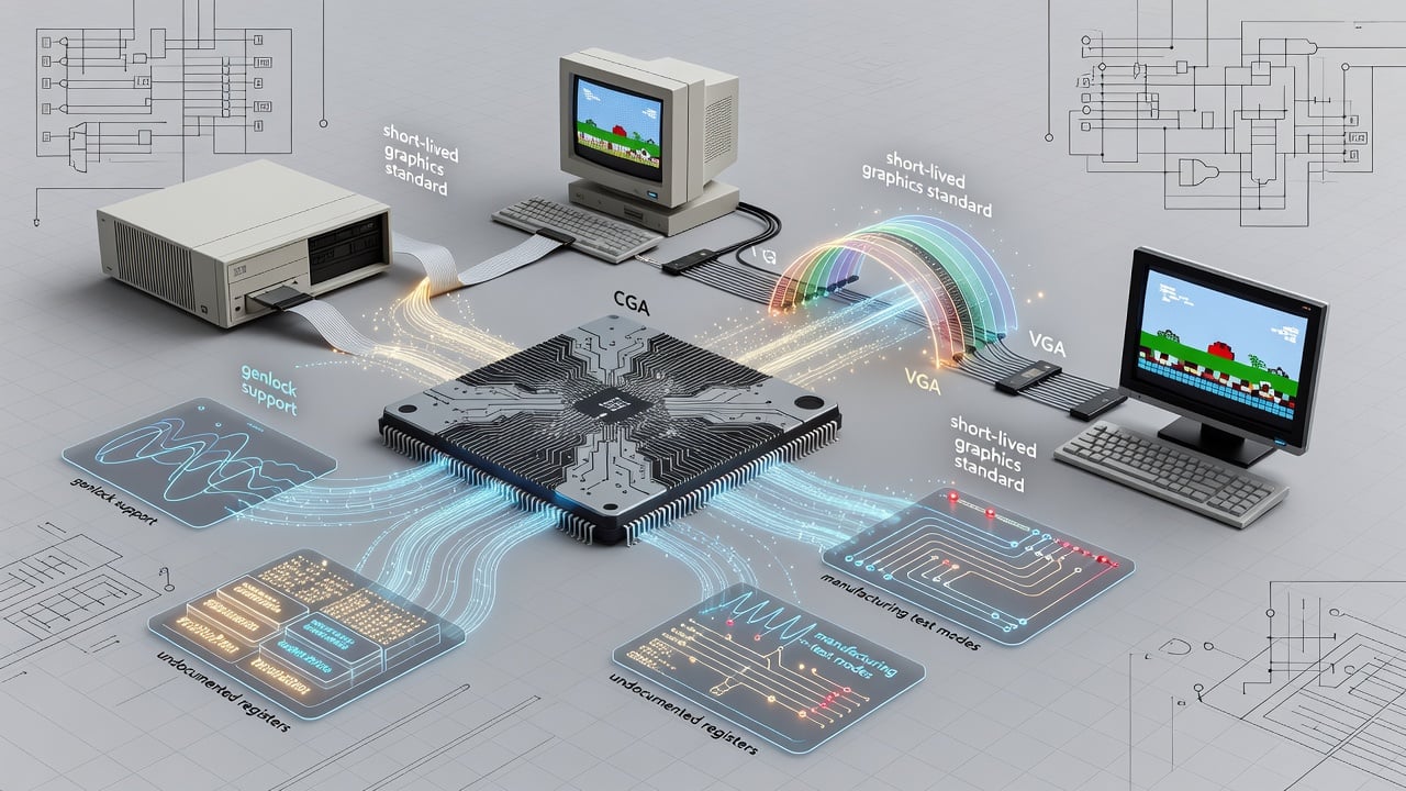
Decades after IBM introduced the Multi-Color Graphics Array with its PS/2 computers, a determined hardware enthusiast has peeled back the layers of its custom gate arrays. The results expose undocumented features, hidden test modes and connections that tie the obscure video chipset to broader graphics history.
Released in 1987 alongside the PS/2 Model 30 and later the Model 25, MCGA served as IBM’s low-cost video solution. It never appeared on standalone cards. Instead it lived on the motherboard. Wikipedia notes that it supported all Color Graphics Adapter modes plus two new ones: 640-by-480 monochrome at 60 hertz and 320-by-200 resolution with 256 colors drawn from an 18-bit palette of 262,144 shades at 70 hertz. No EGA compatibility. No high-resolution color modes that VGA would soon deliver.
Yet that 256-color mode caught on. Game developers embraced it. Titles from Sierra On-Line and Lucasfilm Games mapped their EGA 16-color palettes into the richer MCGA space, leaving many colors unused but gaining smoother visuals. Higher-resolution games often fell back to monochrome or CGA. The standard’s brief life ended when IBM discontinued the Model 25 and 30 by 1990. Epson produced the only known clones in its Equity Ie and PSE-30 systems. VGA, introduced at the same time, simply proved superior.
Now the silicon itself has spoken. Engineer schlae spent months decapping and imaging the two custom gate arrays at the heart of MCGA: the 72X8300 memory controller and the 72X8205 video formatter. Some chips came from IBM’s internal process. Others bore the mark of Seiko. The GitHub repository lays out schematics, KiCad layouts and detailed notes on every basic cell.
The memory controller, implemented in a Seiko SLA6430 with 4,342 basic cells arranged in 167 rows by 26 columns, revealed more than expected. One discovery stands out. MCGA can genlock to external horizontal and vertical sync signals. Pins 11 and 12, normally used for monitor ID readback, double as HSYNC and VSYNC inputs. To activate the mode, software writes a 1 to bit 3 of register 0x12. The PS/2 Model 30 technical reference manual lists that bit as “Reserved = 0.”
Commenters on Hacker News reacted with surprise. One wrote, “A fucking built-in genlock? For years I thought only Amigas had those!” Others speculated why IBM buried the capability. Maybe it supported a canceled project. Perhaps reliability concerns kept it hidden. The genlock pins share duty with monitor ID lines, so the feature appears only on certain builds.
Register 0x10 offers further control. Bit 3 selects a compatibility mode that doubles horizontal timing in 80-column text, adjusting increments and decrements by one. Bit 2 chooses the master clock: 25.175 MHz by default or the 14.318 MHz colorburst frequency. An extended mode register at 0x1A contains two undocumented bits. One may force 256-color operation regardless of resolution. The other could flood the entire display with the border color.
Manufacturing test features fill additional registers. Register 0x20 controls counter speedup by injecting clocks directly into upper or lower bits of internal counters. The video formatter exposes test ports at 0x18 and 0x19 that let engineers read back RAMDAC data, VRAM contents and even 16-color mode information. A write to register 4 can hard-reset the chip or disable all outputs including the RAMDAC.
Reverse engineering followed a painstaking path. Siliconpr0n provided high-resolution die shots. The 72X8300 image, originally over 21,000 pixels square, was scaled and imported into KiCad at a precise factor of 0.10317 to match the 3-millimeter basic-cell spacing. Schlae created custom footprints for each cell type, many of them mirrored or rotated. Two metal layers complicated tracing. Metal 2 carried power and ground rails plus most internal wiring while metal 1 handled horizontal runs. Only specific contacts existed: metal-1 to metal-2, metal-2 to polysilicon gates, and metal-2 to diffusion regions.
Traces started at a pad, followed the metal underneath, connected every related pad to a net, then propagated backward to the schematic. The process reversed normal KiCad flow. The result sits in the repository’s mcga72x8300flat and mcga72x8205flat directories, complete with flattened layouts. Plans call for generating Verilog from the netlist to enable simulation or even FPGA recreation.
But why bother now? Vintage computing communities keep these machines running. The same engineer has released Micro Channel sound cards, EGA card layouts and disk interface adapters. His work fills practical gaps for PS/2 owners who want period-correct peripherals. MCGA’s obscurity created exactly such a gap. Repairing a dead Model 30 often meant sourcing rare parts or accepting degraded video.
Discussions on vintage forums highlight ongoing interest. Threads on Vogons and VCFed document hardware quirks, power-rail shorts and monitor compatibility issues. One recent Facebook post in a Model 25 and 30 group pointed to Twitch streamer TubeTimeUS performing live gate-level reversal of the same chips months earlier. The community effort spans independent researchers sharing decaps, schematics and software patches.
MCGA’s technical compromises reflected IBM’s PS/2 strategy. The company pushed Micro Channel Architecture, proprietary BIOS and analog video at a time when clones dominated the market with cheaper ISA and digital CGA/EGA. MCGA delivered 256 colors cheaply by sharing motherboard real estate and avoiding extra chips. Its palette and connector looked forward to VGA. In practice the subsystem sat between CGA’s limitations and VGA’s full promise.
Software treated it as a special case. Many 256-color VGA titles worked if they avoided multiple video pages or other VGA-only registers. Others shipped dual code paths or simply dropped to CGA. The 640-by-480 monochrome mode found occasional use for sharp text or simple line drawings. Yet the lack of 16-color high-resolution graphics frustrated developers who had embraced EGA.
Today’s findings change the picture. Undocumented registers and the genlock capability suggest IBM considered broader applications than historians recorded. The test modes imply rigorous factory validation of every counter and data path. Those details matter to restorers who need to verify a repaired board or emulate the chipset accurately.
Schlae’s schematics already allow deeper analysis. Future Verilog output could let hobbyists run MCGA logic on modern hardware or debug timing issues in emulators. The Seiko connection adds another thread. Commenters noted that Seiko Epson produced the gate arrays for IBM and also offered the only third-party MCGA systems. Whether licensing, coincidence or quiet partnership remains unclear.
One thing is clear. The chips still hold surprises. Bit 6 in register 0x10 remains marked reserved with unknown effect. The exact behavior of the 0x1A undocumented bits awaits confirmation through testing on real hardware. Manufacturing registers that read internal RAMDAC and VRAM buses could prove useful for diagnostics or even creative video effects.
Vintage hardware enthusiasts continue to extract value from 1980s silicon long after corporate interest faded. IBM moved on to VGA, XGA and beyond. The PS/2 line became a footnote remembered more for its awkward keyboard connector than its graphics. Yet for a small group of dedicated researchers, those gate arrays represent unfinished business.
They pore over die photos. They trace metal lines one cell at a time. And every new connection reveals how IBM balanced cost, compatibility and ambition in a single motherboard chipset. The work doesn’t just preserve old machines. It rewrites small chapters of PC graphics history that everyone thought were already closed.

