
Micro-Quakes on Silicon: How Tiny Vibrations Are Poised to Reshape Mobile Computing
In the relentless pursuit of slimmer, speedier smartphones, engineers at the University of Colorado Boulder have unveiled a breakthrough that harnesses minuscule vibrations akin to earthquakes on a chip. This innovation, detailed in a recent study, promises to compress internal components while enhancing data processing and signal strength. By generating controlled surface acoustic waves—essentially tiny seismic events at the microscopic level—the technology could redefine how devices handle wireless communications, potentially leading to phones that are not only thinner but also more efficient in battery use and performance.
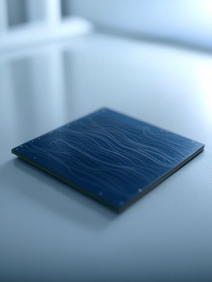
The core of this advancement is a device called a surface acoustic wave (SAW) phonon laser, which operates much like a traditional laser but emits sound waves instead of light. Researchers, led by figures such as Hubert Krenner from the University of Münster and in collaboration with CU Boulder’s team, have managed to create coherent vibrations on a silicon chip smaller than 0.15 square millimeters. These vibrations, oscillating at frequencies up to 1 GHz, are produced using a direct current bias with a threshold as low as 36 volts, yielding an output of -6.1 dBm and a linewidth under 77 Hz. This precision allows for tighter integration of components that traditionally require bulky filters and amplifiers in smartphones.
Unlike conventional radio frequency filters that rely on piezoelectric materials to convert electrical signals into mechanical waves, this new chip uses all-solid-state technology, eliminating the need for moving parts or external stimuli. The result? Devices that can process signals faster without the spatial demands of older hardware. As reported in CU Boulder Today, the team describes it as bottling “the tiniest earthquakes imaginable,” a feat that could shrink the footprint of essential components like antennas and processors.
Unlocking Efficiency Through Phonon Dynamics
Industry experts see this as a game-changer for 5G and emerging 6G networks, where higher frequencies demand more sophisticated signal management. By amplifying surface acoustic waves directly on the chip, manufacturers could reduce the size of bandpass filters, which currently occupy significant space in phone casings. This compression might allow for sleeker designs without sacrificing connectivity, addressing a key challenge in an era where consumers demand ever-thinner devices packed with advanced features like AI-driven cameras and augmented reality.
The technology’s roots trace back to fundamental physics research, building on concepts from quantum mechanics where phonons—quantized units of vibrational energy—can be manipulated like photons in lasers. In practical terms, this means chips that not only generate but also amplify these waves coherently, leading to lower noise and higher fidelity in data transmission. A post on X from The Debrief highlighted how these “artificial earthquake-like waves generated by lasers” could pave the way for more efficient computer chips overall, echoing sentiments in broader tech discussions.
Comparisons to existing innovations underscore its potential. For instance, while China’s recent bismuth-based chips, as noted in posts on X from Alternative News, claim 40% speed boosts and 10% energy savings over silicon, the SAW phonon laser focuses on vibrational precision rather than material substitution. This approach avoids scalability issues plaguing other experimental tech, such as the magnetic helix materials mentioned in X posts by Dr. Singularity, which promise strong electrical responses but remain in early stages.
From Lab Prototypes to Market Realities
Prototyping has shown promising results, with the CU Boulder team demonstrating stable operation under standard conditions. The chip’s ability to produce these waves without mechanical transducers means it could integrate seamlessly into existing semiconductor fabrication processes, potentially using CMOS-compatible methods. This compatibility is crucial for adoption by giants like Qualcomm or Samsung, who dominate mobile chip production.
However, challenges remain. Scaling up production to meet the demands of billions of devices requires overcoming hurdles in material purity and thermal management, as high-frequency vibrations could introduce unwanted heat. Industry insiders point to similar past innovations, like MIT’s energy-efficient microchips discussed in X posts by Mario Nawfal, which aimed at faster devices with longer battery life but faced commercialization delays. The SAW laser’s edge lies in its phonon-based amplification, which might sidestep some of these issues by operating at lower power thresholds.
Further insights come from Digital Trends, which explains how the chip “produces microscopic ‘earthquakes'” to shrink components while boosting signal handling. This aligns with reports from TechXplore, where the device is poised to enable “more sophisticated versions of chips in cellphones and other wireless devices,” potentially accelerating data speeds in crowded spectrums.
Broader Implications for Wireless Ecosystems
Beyond smartphones, the technology holds promise for wearables, IoT devices, and even automotive systems, where space constraints are paramount. Imagine smartwatches with enhanced GPS accuracy or vehicles with streamlined radar systems—all benefiting from miniaturized wave generators. This could disrupt supply chains, reducing reliance on rare-earth elements used in traditional piezoelectric components, thereby easing geopolitical tensions over mineral resources.
Economic factors play a role too. With smartphone sales projected to stabilize after Apple’s 2025 dominance over Samsung, as per PhoneArena, innovations like this could fuel the next growth wave. Analysts anticipate that by integrating such chips, manufacturers might cut production costs by 15-20%, passing savings to consumers or investing in R&D for features like foldable screens or advanced biometrics.
Social media buzz on X, including posts from Science Magazine about earthquake detection via smartphones, underscores public interest in seismic tech applications. While not directly related, it highlights how vibrational sensing is evolving, potentially merging with this chip tech for hybrid uses like real-time environmental monitoring in mobile devices.
Engineering Hurdles and Future Pathways
Despite the optimism, technical barriers persist. Achieving consistent linewidths below 77 Hz at scale demands ultra-precise lithography, a process already strained in the semiconductor industry amid global chip shortages. Collaborative efforts, such as those between CU Boulder and international partners, will be key to refining the design. The device’s -6.1 dBm output, while impressive for its size, may need boosting for high-power applications, prompting research into cascaded amplification stages.
Looking ahead, integration with emerging standards like Wi-Fi 7 or 6G could amplify its impact. As detailed in TechXplore, the phonon laser might enable chips that handle multiple frequency bands more efficiently, reducing interference in dense urban environments. This efficiency could extend battery life by minimizing power draw from signal processing, a boon for always-on devices.
Comparisons to other breakthroughs, such as Delft University’s phonon-splitting chip mentioned in X posts by Mario Nawfal, suggest a converging field where quantum-scale manipulations are becoming feasible. Yet, the SAW laser stands out for its focus on surface waves, which propagate along the chip’s exterior, allowing for easier interfacing with other components.
Industry Adoption and Competitive Dynamics
Major players are already taking note. Apple, with its anticipated 2026 product launches as outlined in Newsweek, might incorporate similar tech to maintain its edge in premium devices. Samsung and Huawei, facing U.S. export restrictions, could leverage this to innovate around sanctions, much like the bismuth chip developments hyped on X.
Adoption timelines hinge on prototyping success. Initial trials, as per CU Boulder Today, show the chip operating stably, but mass production might take 2-3 years. Regulatory approvals for new frequency-handling tech will also factor in, especially in markets with strict electromagnetic interference standards.
The innovation’s ripple effects extend to data centers and AI hardware, where faster signal processing could accelerate machine learning tasks. Posts on X from William Huo about ultra-fast memory chips illustrate the broader push for speed, but the SAW laser’s vibrational approach offers a unique angle by blending mechanical and electronic domains.
Pushing Boundaries in Microscale Innovation
As research progresses, interdisciplinary collaborations will likely accelerate development. Physicists and engineers are exploring hybrid systems combining phonon lasers with photonic circuits, potentially creating chips that handle both light and sound for unprecedented versatility. This could lead to breakthroughs in quantum computing, where stable vibrations are essential for qubit control.
Environmental considerations add another layer. By reducing device size and power needs, this tech supports sustainability goals, cutting electronic waste and energy consumption in manufacturing. Reports from Interesting Engineering emphasize how the “tiniest earthquakes” could shrink and speed up smartphones, aligning with global trends toward greener tech.
Ultimately, this chip represents a pivotal shift in how we engineer mobility. By taming micro-quakes on silicon, it opens doors to devices that are not just smaller and faster, but smarter in harnessing fundamental physics for everyday use. As the field evolves, expect more refinements that could transform not only phones but the entire spectrum of connected technologies.

