
In a fortified complex on the outskirts of Shenzhen, a team of engineers has achieved what U.S. export controls aimed to make impossible: a functioning prototype of an extreme ultraviolet (EUV) lithography machine, the crown jewel of advanced semiconductor manufacturing. This machine, essential for etching the tiniest features on chips powering AI models, smartphones and military systems, was assembled in early 2025 under conditions of utmost secrecy, according to a Reuters investigation. The project, dubbed China’s ‘Manhattan Project’ by insiders, drew on expertise from former employees of ASML Holding NV, the Dutch giant that holds a monopoly on EUV technology.
The prototype occupies nearly an entire factory floor in a high-security laboratory, where workers operated under fake identities to evade detection. Reverse-engineering ASML’s machines formed the core of the effort, with Chinese scientists dissecting imported components and rebuilding them domestically. Huawei Technologies Co. played a pivotal role, providing funding and technical guidance, while the project benefited from billions in state subsidies funneled through China’s National Integrated Circuit Industry Investment Fund, known as the Big Fund.
Reverse-Engineering ASML’s Fortress
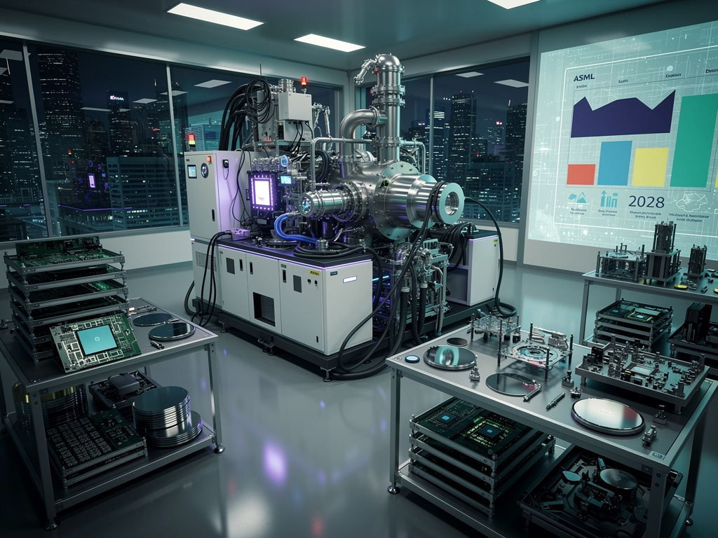
ASML’s EUV systems, which generate light at 13.5 nanometers to print circuits as small as 2 nanometers, rely on a complex interplay of optics, lasers and vacuum chambers. No single company outside the Netherlands produces them, with key parts sourced from German firm Zeiss for mirrors and U.S. supplier Cymer for light sources. Chinese engineers, many ex-ASML staff recruited with lavish incentives, spent years smuggling in older ASML tools and replicating their functions, per the Reuters report. “They have made a prototype EUV machine that works,” one source involved told Reuters, though it has yet to produce viable chips.
Progress accelerated after U.S. restrictions in 2019 barred ASML from selling advanced tools to China, pushing Beijing to invest over $150 billion in semiconductors since 2014. SMIC, China’s largest foundry, has relied on deep ultraviolet (DUV) tools for 7-nanometer chips used in Huawei’s Mate 60 smartphone, but EUV is needed for sub-5-nanometer nodes critical for AI accelerators rivaling Nvidia’s.
The Shenzhen lab’s machine reportedly fires plasma to emit EUV light, bouncing it off multilayer mirrors onto silicon wafers. Testing began in secrecy, with prototypes expected to yield chips by 2028 and mass production by 2030, according to Tom’s Hardware analysis of the Reuters findings.
State-Backed Push Amid Export Siege
China’s effort mirrors the urgency of the U.S. atomic bomb program, with the government allocating $70 billion more for chips atop the Big Fund’s recent $50 billion infusion, as noted in posts on X by industry watcher Kyle Chan. “Secret lab in Shenzhen, team of former ASML engineers, reverse-engineered parts, yet to produce working chips, aiming for 2028-2030,” Chan summarized, linking to Reuters. Alexander NL, another X commentator, highlighted the geopolitical stakes: “China’s EUV prototype could upend the chip wars,” in a post.
Engadget reported that the prototype could power AI chips, underscoring fears in Washington, where officials worry about Beijing’s military applications, from hypersonic missiles to surveillance networks (Engadget). ZeroHedge amplified the story, calling it a direct challenge to Western dominance (ZeroHedge).
Challenges persist: EUV requires ultra-precise engineering, with ASML’s High-NA Twinscan EXE:5000 achieving 8nm resolution after decades of R&D. China’s version lags, using salvaged parts and facing yield issues, but breakthroughs in domestic laser-produced plasma sources, pioneered at Tsinghua University since 2021, offer a path forward, as Chan noted in earlier X threads.
Global Ripples and Western Countermeasures
The U.S. Commerce Department’s Bureau of Industry and Security has tightened rules, verifying ASML shipments and probing ex-employee hires. In October 2025, new controls targeted 140 Chinese firms, including those linked to EUV research. Yet, reports from Wccftech suggest China’s prototype marks a ‘semiconductor breakthrough the U.S. has feared,’ potentially enabling SMIC to hit 5nm by decade’s end without foreign tools.
Europe faces dilemmas: ASML, valued at over €300 billion, derives 40% of revenue from China via DUV sales. Dutch and U.S. pressure led to a 2025 export license halt for advanced EUV, but maintenance for existing machines continues, providing reverse-engineering fodder. ITdaily described it as a ‘Manhattan Project in the Far East,’ with the prototype essential for modern microchips (ITdaily).
NotebookCheck detailed that the machine isn’t fully functional yet, projecting mass production in 2028-2030, reliant on ex-ASML talent (NotebookCheck). TrendForce noted use of older ASML components, eyeing 2028 chipmaking (TrendForce).
Path to Chip Autonomy
Huawei’s involvement signals integration with China’s AI ambitions; its Ascend 910C chips, built on 7nm, already compete in domestic data centers. EUV success could propel them to 3nm parity with TSMC. Cryptopolitan called it a ‘new chapter’ in the semiconductor fight (Cryptopolitan). IOPLUS framed it as an ‘all-or-nothing race’ for independence, questioning 2030 viability (IOPLUS).
For industry insiders, the prototype’s viability hinges on scaling: power consumption exceeds 1 megawatt per tool, and defect rates must drop below 0.1 per wafer. Yet, China’s command economy—mobilizing 10,000 engineers, per Reuters sources—contrasts with ASML’s open innovation, potentially accelerating iteration.
As testing proceeds in Shenzhen’s shadows, the chip world’s balance teeters. Western firms watch warily, pondering if export walls can hold against Beijing’s relentless drive.

