
For decades, spectral imaging has operated under a simple but costly paradigm: capture first, analyze later. Hyperspectral cameras mounted on satellites, drones, and laboratory instruments collect enormous volumes of data across hundreds of wavelengths of light, then transmit that data to powerful computers for processing. The result is a bottleneck that limits real-time decision-making and consumes vast amounts of energy and bandwidth.
Now, a team of researchers at Lawrence Berkeley National Laboratory has upended that model with a first-of-its-kind sensor that doesn’t just capture spectral images — it simultaneously identifies targets of interest using artificial intelligence embedded directly into the hardware. The device, which the team describes as a sensor that “sniffs out” spectral signatures, represents a fundamental shift in how machines perceive and interpret the world around them.
A Sensor That Thinks as It Captures
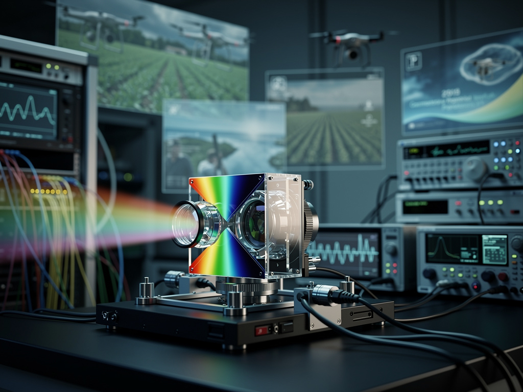
The breakthrough, detailed in a paper and announced by Berkeley Lab’s news center, centers on a novel integration of optical hardware and machine learning. Traditional hyperspectral imaging systems work sequentially: a detector array captures light across many wavelengths, producing a data cube — a three-dimensional block of information combining spatial and spectral dimensions. That cube is then shipped off for post-processing, where algorithms sift through it to identify materials, chemicals, or biological markers based on their unique spectral fingerprints.
The Berkeley Lab sensor collapses these two steps into one. By encoding AI classification capabilities directly into the sensor’s physical architecture, the device can recognize predefined spectral targets at the moment of detection — no downstream computation required. According to the Berkeley Lab announcement, this is the first demonstration of a smart spectral sensor that performs inference simultaneously with data acquisition, a capability the researchers liken to a biological nose that identifies a scent the instant it is encountered.
How the Hardware Encodes Intelligence
The technical achievement rests on a concept known as optical computing, in which the physical properties of light — its wavelength, phase, and amplitude — are manipulated by carefully designed optical elements to perform mathematical operations that would otherwise require electronic processors. In this case, the sensor’s optical front end is engineered so that incoming light is transformed in a way that maps directly onto a trained neural network’s classification weights.
In practical terms, the sensor uses metasurfaces or diffractive optical elements — precisely patterned structures smaller than the wavelength of light — to sort and weight incoming photons according to spectral features that distinguish one target material from another. The result at the detector plane is not a raw image but a pre-classified signal: a direct readout of whether a target of interest is present. The Berkeley Lab team reported that the sensor achieved high classification accuracy across multiple spectral targets, rivaling software-based approaches while operating at a fraction of the power and latency.
Why Speed and Efficiency Matter at the Edge
The implications are most profound for applications where data must be acted upon immediately and where bandwidth or power is severely constrained. Consider a satellite orbiting Earth, tasked with monitoring agricultural health, detecting wildfires, or identifying chemical spills. A conventional hyperspectral satellite generates terabytes of data per day, most of which must be downlinked to ground stations before any useful information can be extracted. This creates delays of hours or even days between observation and action.
A sensor with built-in AI classification could flag critical events in real time, transmitting only the relevant alerts rather than the full data stream. The reduction in data volume could be orders of magnitude, dramatically lowering communication costs and enabling faster response times. The same logic applies to unmanned aerial vehicles surveying disaster zones, autonomous vehicles navigating complex environments, and portable medical devices screening tissue samples for disease markers in resource-limited settings.
The Convergence of Photonics and Machine Learning
The Berkeley Lab work sits at the intersection of two rapidly advancing fields: nanophotonics and edge AI. Over the past several years, researchers worldwide have been exploring ways to offload computation from electronic chips to optical systems, motivated by the fundamental speed and energy advantages of photonic processing. Light travels faster than electrical signals, generates less heat, and can carry information across many channels simultaneously through wavelength multiplexing.
At the same time, the AI community has been pushing to shrink neural networks small enough to run on edge devices — smartphones, wearables, IoT sensors — rather than relying on cloud servers. The Berkeley Lab sensor takes this miniaturization to its logical extreme: the neural network isn’t merely small enough to fit on a chip; it is physically instantiated in the optics themselves. There is no chip running inference. The physics of light propagation is the inference.
Potential Applications Spanning Multiple Industries
The range of potential use cases for such technology is vast. In agriculture, spectral sensors mounted on drones already help farmers assess crop stress, nutrient deficiencies, and pest infestations. But current systems require post-flight data processing. A smart spectral sensor could provide real-time field maps during the flight itself, enabling immediate intervention. In environmental monitoring, the technology could be deployed to continuously scan waterways or industrial sites for pollutant signatures, triggering alarms the moment a hazardous chemical is detected.
In defense and security, spectral identification of materials — including explosives, chemical agents, and camouflaged objects — is a well-established capability, but one that has historically required bulky equipment and significant processing power. A compact, self-classifying sensor could be integrated into handheld devices or small autonomous platforms, extending spectral intelligence to the tactical edge. In healthcare, rapid spectral classification of tissue could accelerate surgical decision-making or enable point-of-care diagnostics in clinics without access to laboratory infrastructure.
Challenges on the Road to Deployment
Despite its promise, the technology faces significant hurdles before it can be widely deployed. One challenge is flexibility: because the AI classification is physically encoded in the sensor’s optics, the device is optimized for a specific set of targets. Changing the classification task may require redesigning and refabricating the optical elements, unlike a software-based system where a new model can be loaded in seconds. The Berkeley Lab team acknowledged this trade-off, noting that the current approach is best suited for well-defined, mission-specific applications where the targets of interest are known in advance.
Manufacturing scalability is another open question. The metasurfaces and diffractive elements that encode the neural network must be fabricated with nanometer-scale precision, a process that is well-established in research cleanrooms but has yet to be proven at commercial volumes. However, advances in semiconductor lithography and nanoimprint techniques are steadily closing this gap, and several photonics foundries are actively developing platforms for mass production of complex optical structures.
A Broader Push Toward Intelligent Sensing
The Berkeley Lab sensor is part of a broader movement in the scientific and engineering communities toward what some researchers call “intelligent sensing” or “computational sensing” — the idea that sensors should not be passive data collectors but active participants in the interpretation of the signals they receive. This philosophy challenges the traditional separation between sensing and computing, arguing that the two functions can and should be co-designed for maximum efficiency.
Other research groups have demonstrated related concepts, including optical neural networks for image classification and programmable photonic processors for signal analysis. What distinguishes the Berkeley Lab work, according to the team’s announcement, is the tight integration of spectral imaging with target classification in a single, compact device — a combination that had not previously been achieved.
What Comes Next for Smart Spectral Hardware
Looking ahead, the Berkeley Lab researchers indicated interest in expanding the sensor’s capabilities to handle more complex classification tasks and a greater number of target classes. They are also exploring ways to make the optical encoding reconfigurable, potentially using tunable materials or programmable metasurfaces that could be adjusted in the field to adapt to new missions.
The work underscores a fundamental truth about the future of sensing technology: as the volume of data generated by sensors continues to grow exponentially, the ability to extract meaning at the point of collection — rather than after the fact — will become not just advantageous but essential. Berkeley Lab’s AI-powered spectral sensor offers a compelling glimpse of that future, one in which the boundary between seeing and understanding dissolves entirely.

