
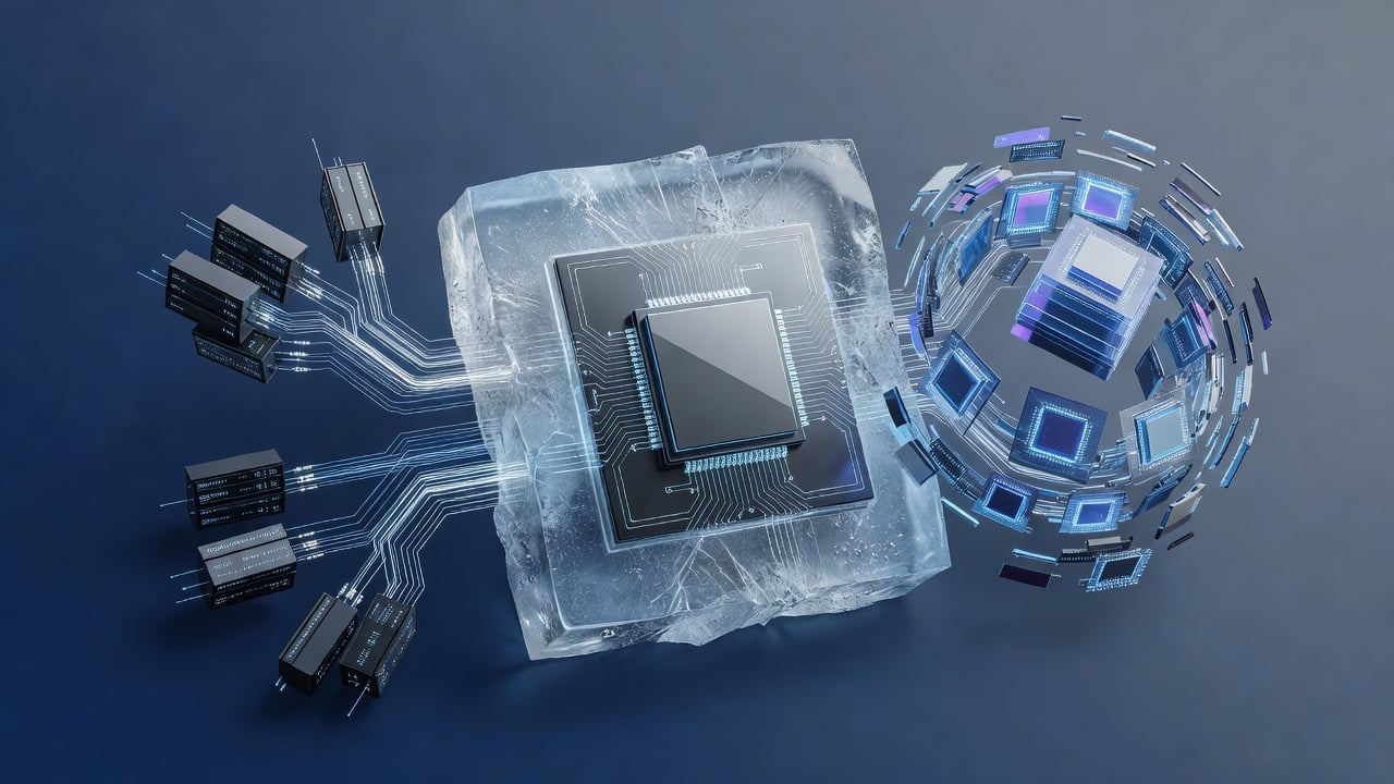
Google has a problem shared by every major AI builder. It cannot get enough chips or power to meet demand for its models. So the search giant is exploring an unusual fix. It wants to etch parts of its Gemini AI directly into custom hardware.
The project carries the internal code name Frozen v2. According to a report from The Information, the new silicon could deliver six to 10 times better efficiency than Google’s current tensor processing units when measured in tokens produced per watt. Alphabet shares jumped as much as 3.7 percent after the story broke Monday.
But this is no quick win. Deployment sits years away, with a target of 2028 at the earliest. And the approach trades flexibility for raw speed and lower costs. That bargain carries real risks in a field that changes by the month.
Here’s how it works. Standard AI chips keep neural network weights in high-bandwidth memory. Data shuttles constantly between compute units and that memory. The back-and-forth eats power and adds latency. Frozen v2 flips the script. It hard-wires Gemini’s current architecture straight into the circuitry itself.
Engineers could still update the model weights. Yet the underlying structure stays fixed. Or frozen. The result looks less like a general-purpose accelerator and more like a purpose-built engine for one family of models. The Next Web described it as a chip that becomes the model.
This idea did not emerge from nowhere. Google already pours billions into its TPU lineup. The latest generation, announced in April, includes separate chips for training and inference. TPU 8t targets high-throughput model development. TPU 8i focuses on low-latency reasoning needed for agentic systems. Bloomberg covered the launch in detail.
Those TPUs help Google reduce dependence on Nvidia GPUs. They also power much of Google Cloud’s AI offerings. Demand still outstrips supply. Internal shortages have grown so acute that the company capped access for some paying customers, including Meta, according to recent reports. The pressure explains why Frozen v2 exists as a complement rather than a replacement.
Efficiency gains of that magnitude would matter at data-center scale. Each percentage point saved on power or memory bandwidth translates into millions of dollars when thousands of chips run around the clock. Faster inference also improves user experience for real-time applications such as voice assistants or coding tools. Lag becomes the enemy.
Yet the timing looks awkward. Google already faces criticism over delays in its Gemini lineup. Just last week, the Los Angeles Times detailed months-long slippage on Gemini 3.5 Pro. Engineers cited disappointing coding performance even after the team refreshed training data in late June. Internal frustration runs high. Ten current and former employees told reporters the company risks falling behind Anthropic and OpenAI.
Those software troubles could complicate hardware bets. A chip built around today’s Gemini architecture might feel obsolete by the time it reaches production. Model designs evolve quickly. New architectures appear regularly. Hard-wiring one version locks in assumptions that might not hold.
Google appears aware of the hazard. The Frozen approach reportedly leaves some room for weight updates. Still, the core topology remains set in silicon. That rigidity echoes a broader debate inside the industry. How much customization makes sense when progress moves at breakneck speed?
Others have reached similar conclusions. A startup called Taalas already ships chips with models such as Llama 3.1 8B baked directly into the silicon. The company claims inference speeds up to 17,000 tokens per second. No expensive high-bandwidth memory required. Discussions on X this week drew direct parallels between Taalas’ Hardcore chips and Google’s Frozen v2.
One post from AI analyst accounts noted the shared philosophy. The model becomes the chip. Extreme efficiency follows. But so does potential brittleness if the frozen design falls behind newer approaches.
Google has declined to confirm Frozen v2. A spokesperson told reporters the company constantly experiments with high-efficiency concepts. Not every prototype reaches customers. That careful language fits a pattern. Alphabet rarely discusses unreleased hardware until it reaches production readiness.
The project still sent a clear signal to investors. Alphabet shares climbed on the news. Analysts have long viewed Google’s custom silicon as a hidden advantage. Bloomberg argued last year that success with TPUs helped drive a 30 percent rally in the stock. A specialized Gemini chip could amplify that edge.
Wall Street sees the possibility of a $900 billion boost to Alphabet’s valuation from its AI infrastructure bets. Those numbers assume the company can solve its capacity problems without simply buying more Nvidia hardware at premium prices. Frozen v2 offers one path toward that independence.
Memory constraints add another layer. The AI sector already faces a looming shortage of high-bandwidth memory. Chips that reduce reliance on that resource become doubly attractive. Google has spread its orders across multiple suppliers, including Intel and TSMC, to hedge risks. A design that sidesteps some memory needs would fit neatly into that strategy.
But challenges remain. Fabrication at scale takes years. Testing a chip with hard-wired neural architecture requires new validation methods. And the competitive picture grows more crowded. Nvidia continues to dominate the market for training GPUs. Rivals such as AMD just unveiled their own rack-scale systems to challenge that lead.
Google’s bet also highlights a shift in thinking about AI infrastructure. For years the focus stayed on bigger clusters and faster interconnects. Now companies hunt for architectural shortcuts that squeeze more performance from each watt. Specialization at the silicon level represents the next logical step.
Whether Frozen v2 reaches deployment in 2028 depends on many factors. Model progress between now and then could render the current Gemini design less relevant. Internal engineering priorities might shift if software delays persist. And the economics must justify the upfront investment in a new chip line.
Even so, the mere existence of the project reveals how seriously Google takes its compute constraints. The company that helped popularize large-scale machine learning now searches for ways to make its flagship model run cheaper and faster than anyone else’s. That search has led it to consider etching the model itself into metal.
Success would reshape the economics of running Gemini at planetary scale. Failure would simply add another interesting footnote to Google’s long history of ambitious hardware experiments. Either outcome carries lessons for the rest of the industry.
One thing looks clear. The era of purely general-purpose AI accelerators may be giving way to a hybrid future. Some workloads will still need flexible GPUs or TPUs. Others could benefit from silicon that knows its model by heart. Google wants to own both sides of that equation.


 WebProNews is an iEntry Publication